
The CD4094 IC is a CMOS IC designed for serial to parallel data conversion and output latch control. This article explains the CD4094 shift register circuit, pin configuration, and internal logic circuit of this 8-bit register. It also covers how CD4094 IC works, practical applications, and how to interface it with microcontrollers like Arduino.
From LED control to data expansion, engineers use this serial output register for flexible digital signal management. Explore its data latch, timing, and control signal operations in detail, including a comparison between CD4094 vs 74HC595. Whether building a display driver or expanding I/O ports, understanding this logic control IC helps in designing reliable digital electronics projects.
Introduction
In the world of digital electronics, the need for efficient data handling is constant. The CD4094 IC has earned its place among the most versatile components used for serial to parallel data conversion. It belongs to the CMOS IC family and is best known for converting serial data streams into parallel output for controlling multiple devices simultaneously.
This 8-bit register makes it easier for engineers to manage complex logic circuits, especially when using microcontrollers with limited I/O pins. Commonly referred to as IC4094, this component integrates functions like a data latch and output latch to provide stable signal storage.

The CD4094 shift register circuit finds its way into display systems, LED matrices, and data bus extensions, where output expansion is essential. Let’s dive deeper into its structure, functionality, and practical use in various electronics projects.
What is CD4094 IC?
The CD4094 IC is an 8-bit shift register with serial output and parallel output capabilities. It can store and shift data with high precision using low-power CMOS technology. This device is often used as a serial to parallel converter using CD4094, which makes it a popular choice in control systems, especially in automation and microcontroller-based designs.
This IC contains a data latch for holding temporary information and an output latch for maintaining stable logic levels at the outputs. The data shift operation occurs on every clock pulse, transferring the serial input data through its internal flip-flops until it appears at the register output.
Internally, the logic circuit of this IC ensures that once data is latched, it remains unchanged until a new control signal (strobe or enable) is applied.
Key features include:
8-bit data storage and shifting
Independent output enable control
Low power consumption due to CMOS IC design
Cascading capability for multiple output stages
Pin Configuration and Description
Understanding the CD4094 pin configuration and datasheet is essential for accurate circuit design. This IC comes in a standard 16-pin dual in-line package (DIP), which is widely used on breadboards and PCBs.

Pin Functions:
DATA IN (Pin 2) – Accepts the serial data input.
CLOCK (Pin 3) – Receives the clock pulse to shift the data.
STROBE (Pin 1) – Acts as the control signal for the output latch.
OUTPUT ENABLE (Pin 15) – Controls the activation of parallel output lines.
Q1–Q8 (Pins 4–11) – Provide parallel output signals for 8-bit data.
SERIAL OUT (Pin 9) – Sends the last bit of data for cascading to another IC.
VDD (Pin 16) – Power supply (3V to 15V typical).
GND (Pin 8) – Ground connection.
This configuration enables engineers to design systems that can easily cascade CD4094 ICs for multiple outputs, allowing for extended data control beyond 8 bits.
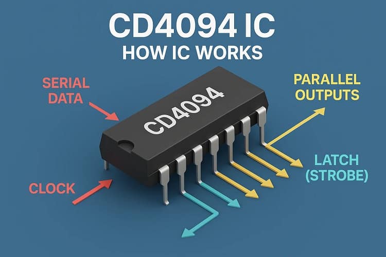
Working Principle of CD4094 IC
To understand how CD4094 IC works, it helps to imagine it as a pipeline transferring bits step by step with each clock pulse. The data enters through the serial data input and shifts through the internal stages until it fills all eight flip-flops in the 8-bit register.
Each bit moves forward on the rising edge of the clock pulse, while the strobe signal (often referred to as the data latch control) determines when the data is transferred to the parallel output pins.
When the output enable signal is active, the stored bits appear on the output terminals, making it ideal for LED control using CD4094 IC. This approach allows multiple LEDs or display elements to operate synchronously without interfering with one another.
In automation or display applications, engineers often interface CD4094 with Arduino to expand the output capabilities. The Arduino interface handles serial communication, while the IC manages the output latch for stable, flicker-free performance.

Core Working Steps:
Serial data is fed into DATA IN.
Each clock pulse shifts the data through the internal flip-flops.
The strobe signal latches the data to outputs.
The output enable line activates the stored pattern on LEDs or devices.
This mechanism makes it an effective serial to parallel converter using CD4094 for controlling multiple devices using only a few microcontroller pins.
Applications of CD4094 IC
The applications of CD4094 shift register are widespread in both educational and industrial projects. Some of the most common uses include:
LED driver circuit for display and indication systems
Serial to parallel data conversion
Output expansion for microcontrollers
Logic control IC in embedded systems
Data bus extension in automation hardware
Cascading CD4094 ICs for multiple outputs to control complex lighting or relay modules
In advanced designs, engineers often prefer CD4094 vs 74HC595 comparison to choose the most efficient option for power, speed, and voltage compatibility.
Advantages and Limitations
Advantages
Uses CMOS IC technology for low power operation
High noise immunity and wide voltage range
Supports output enable and output latch control
Easy to interface CD4094 with Arduino for automation
Can cascade for multiple serial output stages
Limitations
Slower than TTL-based registers like 74HC595
Sensitive to timing mismatches in the clock pulse
Limited current driving capability, requiring external transistors for heavy loads
Despite these limitations, the CD4094 shift register circuit remains one of the most reliable and efficient options for signal expansion and display control in modern electronics.
People Also Ask
What is CD4094?
The CD4094 is an 8-bit shift register with both serial output and parallel output, designed for serial to parallel data conversion. It uses CMOS IC technology for low power and high reliability.
What is the IC number of 4-bit shift register?
A common 4-bit shift register IC is IC 7495, which performs similar data shifting functions but on four bits instead of eight.
What is the use of CD4017 IC?
The CD4017 IC is a decade counter used to drive LED chasers and sequencing circuits. It differs from CD4094 because it counts rather than shifts data.
What is IC 74194?
The IC 74194 is a bidirectional universal shift register that allows shifting of data in both directions — left and right — offering greater flexibility in logic circuit design.
Conclusion
The CD4094 IC continues to be an essential component in digital electronics projects requiring serial to parallel data conversion. With its 8-bit register, output latch, and control signal versatility, it serves as a bridge between serial communication and real-world hardware outputs. Whether used in LED displays, automation systems, or experimental setups, this CMOS IC offers reliability and simplicity.
For more related circuit ideas and interfacing tutorials, visit SekhoHub.online — your hub for DIY electronics and detailed guides on logic and microcontroller-based circuits.